ASML is one of the most important companies in the semiconductor world. If it magically evaporated overnight, all over the world, all construction of the most advanced chip factories would be completed firstand then, over time and the growing problem of lack of spare parts, all existing factories producing the latest AI accelerators, processors for smartphones, laptops and the fastest types of computer memory would cease to exist. The world of electronics as we know it would simply cease to exist and it would take years to rebuild it. This is because ASML is the only manufacturer of key machines used in the production of cutting-edge chips, i.e EUV lithography systems.
The rest of the article is below the video
ASML, i.e. specialists in light sculpting in silicon
Manufacturing a processor for the latest iPhone, for example, is an incredibly complicated process. Before it is cut from a silicon wafer, packaged and soldered to the motherboard of the target device, it goes through hundreds of subsequent stages of the production process, which can take up to several months. During this time, he goes several times to one of the key, and certainly the most expensive, machines in the factory, i.e EUV system, which acts as a matrix “embossing” the pattern of the processor's internal connections on the wafer surface.
In this machine, a silicon wafer covered with a substance called photoresist is exposed to light (hence the “lithium” in the name lithography) of a precisely selected wavelength. On the way from the light source to the wafer, the light meets the mask, which has a pattern with the connections that are to be created in the manufactured chip, so a mesh of lights and shadows reaches the wafer. The light activates the photoresist on the wafer, which – depending on the substance used – either causes it to interact with the substrate (you can think of this process as light-curing seals) or prevents it from interacting with it. The inactive photoresist is then removed and a thicket of lines with a width measured in nanometers remains on the wafer.
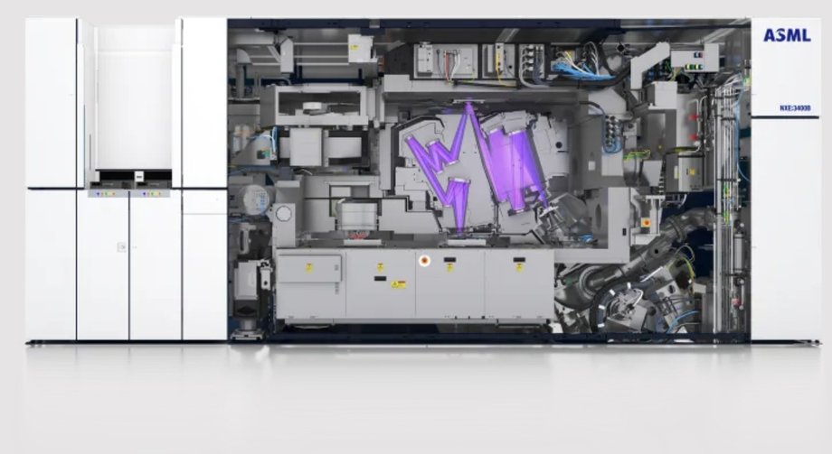
ASML's EUV lithography system is required to print all of the world's most advanced semiconductors
|
ASML
The simple rule is that the shorter the wavelength of light used in a lithography machine, the denser the network of connections it can create. This, in turn, translates directly into the performance of the chip being created. ASML is the only company with the technology to use EUV light (Extreme Ultraviolet) with a wavelength of 13.5 nm. For comparison, earlier generation machines, produced not only by ASML but also by Nikon, use light with a wavelength of “as much as” 193 nm.
ASML solutions at the intersection of technology and magic
What does this mean? Let's focus on two key elements of these machines. Firstly, A huge problem that has cost billions of dollars over the years has been to create a sufficiently efficient light source. Sufficiently efficient, i.e. one that can be used for mass production of chips, and not for irradiating individual wafers in the laboratory. To put it simply, inside 60,000 are fired every second. drops of tin and each of them is hit twice by a laser beam in flight. The tin turns into plasma and emits light. If this sounds unbelievable, well, welcome to the world of semiconductor manufacturing, where the line between technology and magic is very fluid.
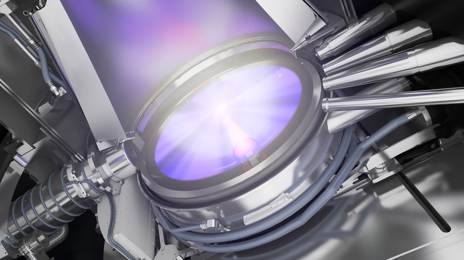
ASML machines generate light by shooting a laser at tin droplets.
The second impressive feature of the EUV machine is its optical system. It is composed of a set of mirrors manufactured by the German company ZEISS. In the latest generation of ASML systems, the largest one is 1.2 m in diameter, weighs 360 kg, has over 100 layers and is one of the smoothest objects in the world. A representative of ZEISS once said that if one of the mirrors of the latest generation EUV machine were enlarged to the size of the surface of Germany, the largest irregularity on it would be the thickness of a human hair. The production process of such mirrors takes almost a year. Currently there is no company that could replace ZEISS, which cooperates closely with ASML.
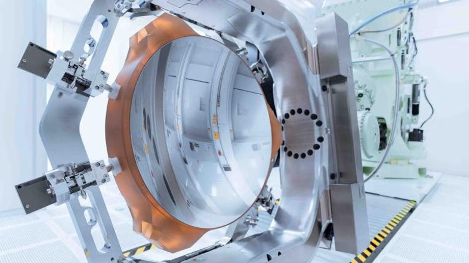
The mirrors used in ASML machines are manufactured in a similar way to mirrors for space telescopes.
In short, the latest generation of EUV systems cost $350-400 million for a reason. They are just that the most advanced mass-produced machines in the history of the world. Another obstacle to copying them is the fact that they are controlled by incredibly complex software. ASML's position is additionally secured by the fact that, due to the key importance of its machines, a global technological ecosystem of connected vessels worth billions of dollars has been created around them, which is very difficult to “settle” and convince to change.
Potential competitors: none at all
Currently Competitive EUV systems would be easiest for the Japanese Nikon to createwhich is the only major manufacturer of lithography machines outside of ASML and experimented with extreme ultraviolet at the beginning of the last decade. Japan also produces many of the key chemicals and other complex machinery used in the chip production process. However, this venture would require support from the Japanese government, academia, business and billions of dollars in investments at various points in the supply chain. For now, there is no indication that anything like this will happen.
However, we know that secret laboratories in China are working feverishly on this type of technology. As a result of sanctions imposed on this country by the US, Chinese factories cannot buy ASML systems, which effectively cut off the Chinese from producing the most advanced chips on their own. Chinese engineers are doing everything they can to recreate machines from the Netherlands using reverse engineering and other more or less legal solutions. According to recent reports, they have already managed to create a basic prototype of this type of equipment that generates light of the necessary wavelength, but which cannot yet be used to expose wafers. In their favor is the fact that the machine created by China would not have to have commercial value and would be used even if it was drastically inferior to ASML equipment in terms of capabilities and performance. However, even if they manage to create such a system and build the necessary ecosystem around it, it will take years to work on.
ASML is benefiting from the AI boom
The challenge for ASML, although this company is key to the entire semiconductor market, is a limited number of potential recipients of its products who do not invest in expanding factories if they do not have to do so. After the rapid increases in value recorded during the pandemic, when the technology world experienced a chip shortage, investor enthusiasm for ASML clearly cooled down when the market stabilized and it turned out that although the company's production capacity was reserved for years in advance, it had no major growth prospects.
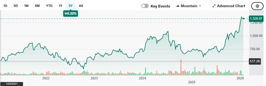
ASML's stock valuation is currently at record highs.
|
Onet
Shortly thereafter, however, the AI boom came Currently, the world is once again facing a chip shortage. Many companies assume that this time we are not dealing with a cycle of demand growth typical of this market, which will soon return to the old level, but a new reality in which chip production must be significantly increased permanently. Therefore, chip manufacturers, historically reluctant to invest in new factories, have decided to significantly increase their processing capacity in the coming years, which in turn means a significant increase in demand for ASML products. This is why, after the last financial report of TSMC, during which the company announced record investments in new factories, ASML's capitalization increased and exceeded the historical value of USD 0.5 billion.
ASML's geopolitical stride
The second challenge for ASML is geopolitics, which is now inextricably linked to chip production. This semiconductor monopoly stands at a geopolitical crossroads between the USA and Europe. Although the company's headquarters is located in the Netherlands, There are several ASML companies operating in the USAdealing with, among other things, research and production of light sources for lithographic systems, which is one of their key elements. They are based largely on US intellectual propertyobtained by ASML as a result of the acquisition of the American companies SVG in 2000 and Cymer in 2013. This is why, when the US began to impose technological sanctions on China, ASML had to adapt to them.
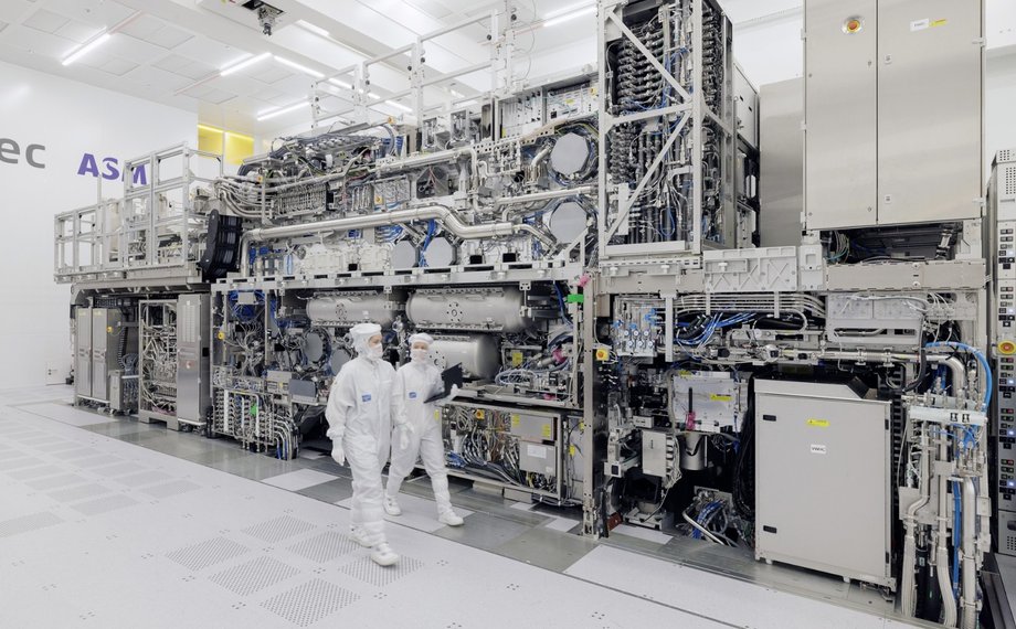
ASML's “extreme ultraviolet” system, used in semiconductor production
|
ASML
On the one hand, this geopolitical divergence means that ASML should rather avoid possible more drastic export regulations imposed by the USA and the European Union. The “halves” of this company located on both sides of the Atlantic cannot exist without each otherso if one of them were somehow blocked or subject to high tariffs, it would be a form of self-sabotage. On the other hand, if someone decided to use such a nuclear option, no one would ever doubt that ASML is one of the most important companies in the world.