During the scientific conference held in Shanghai, Huawei presented quite an earthquake to the world of technology through the mouth of He Tingbo, the head of the company's semiconductor department. The Chinese giant first joined the team trying to bury the so-called Moore's Law, which has set the pace for the entire semiconductor industry for years, claims that has something better, i.e. the so-called τ scaling (tau).
Then he announced that despite the lack of access to the latest lithography machines, a key stage of chip production, he would be able to achieve transistor packing density within a few years. comparable to Intel and TSMC's future 1.4nm manufacturing processes.
It's easy to see why these assurances caused quite a stir. Some media and analysts hailed Huawei's presentation as a new “DeepSeek moment”. People often talk about the technological revolution, the ineffectiveness of sanctions, etc. on the Internet. Traditional practice turns out to be much more nuanced.
Huawei promises a revolution in chip production
Let's start with a general overview of what Huawei has presented and what the company claims about it, and then we will break it down and discuss what is a revolution and what is just an inflated marketing balloon.
As I mentioned, one of the main elements of the breakthrough described by Huawei is the idea of the so-called τ scaling. The Chinese giant argues that further progress on the semiconductor market should be measured not only by how many transistors can be crammed onto a silicon wafer, but above all by how much the operation time can be shortened. That is kind of wants to replace mm² with seconds.
Huawei rightly notes that focusing solely on the size of transistors makes very little sense.
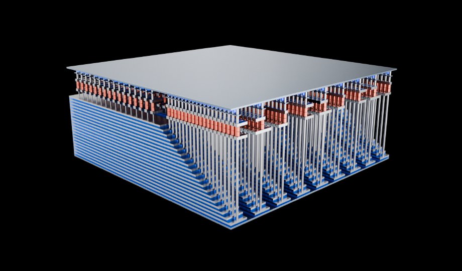
The second important element of Huawei's announcement is LogicFolding technologywhich is intended to allow the company to achieve the previously mentioned breakthrough in the field of chip production and bypass restrictions resulting from sanctions. To put it simply, LogicFolding is a solution in the field of the so-called three-dimensional advanced semiconductor packaging allowing the construction of multi-story chips.
Huawei claims that The company's latest smartphone processor from the Kirin family has two levelsi.e. in practice, one part is created on one wafer, the other on the other, and then they are “glued” together using a technology called hybrid bonding. Future generations of chips are to have even more levels, which is where the statement comes from that in the future Huawei chips will have approximately as many transistors on each square millimeter of surface as chips produced in the latest technological processes of TSMC, Samsung or Intel, which currently scale in two dimensions.
In addition to increasing the number of transistors per chip surface, this solution is intended to increase chip efficiency, because in some cases it allows for shortening the internal paths in the chip, because the signal can also travel through a potentially much shorter vertical connection.
The Chinese with new impressive technologies
So much theory. Let's start with the positives. Huawei is generally right that focusing only on nanometers and the transistor count of chips makes less and less sense. Especially in today's era dominated by AI-related calculations and giant computing clusters that perform them, the importance of a single chip is constantly decreasing and a systemic approach to the topic is becoming more and more important.
Huawei's announcements related to new processors also look very impressive. If this company and its partners managed to achieve such an advanced technology of “gluing” chips that it allows de facto to combine the final processor from two parts, it is a huge breakthrough. The head of Huawei's semiconductor department mentioned that already this year, the company's new processors will in practice use hybrid bonding with a raster (i.e. the distance from the center of one “hole” in silicon with a copper connection to the center of the second “hole”) of 1.5 μm. For comparison, the versions of this technology currently used on an industrial scale in the Intel and TSMC portfolio have a raster size of 9–10 μm, and The decline to the level presented by Huawei was to take place only in a few years. Moreover, although stacking chips on top of each other has been a fairly common practice for several years, doing so in the way Huawei talks about outside of China remains in the realm of research and announcements.
YMTC, the Chinese champion of memory production, is one of the leaders in hybrid bonding technology, which is widely used in the production of NAND memory. It is likely that this company worked with Huawei and SMIC to develop the solutions described by Huawei.
There are other interesting implications of this announcement. First, if Huawei's announcements reflect real progress in China's entire advanced packaging ecosystem, it would be good news also for Chinese producers of RAM and NAND memory. In the case of these types of semiconductors, the technology of “gluing” wafers is already very important today. In some applications, at least as important as access to machines that allow you to create smaller transistors.
This is too interesting information about the state of the Chinese software ecosystem. It is rarely talked about, but the sanctions limit the Chinese not only access to equipment, but also to specific CAD applications in which processors are created. Tools of this type from American leaders, i.e. Synopsys and Cadence, are just beginning to support the design of “three-dimensional” chips. However, Huawei claims that the applications used by the company's engineers are already quite developed in this respect. It is impossible to verify these assurances, but in this case the possibility of Chinese companies catching up the distance would not be as unlikely as in the case of lithography.
The problem is not with technology, but with marketing
In short, Huawei really has something to be proud of and if the assurances just described are true, the engineers of this company and its partners deserve respect. The problem, however, is that Huawei is still Huawei.
The main problem with Huawei's τ scaling is that… it is nothing new. The industry has been wanting to bury Moore's Law for years (now, like Schrödinger's cat, it is both alive and dead at the same time), or at least says that it now means something completely different than it used to. Everyone also realizes that transistor scaling has slowed down and that making every transistor count is more and more important than counting transistors.
Close cooperation between chip designers and factories and optimization of connections inside chips has also been the market standard for at least several years. Whereas is a leader in systemic thinking about computing power Nvidiawhich owes its current market position largely to him. In short, nihil novi. Huawei simply gives these frameworks a common name and thus tries to steer the narrative — probably also to distract attention from the fact that the company's equipment would be even better if it combined various types of optimizations with the ability to produce smaller transistors.
Nvidia owes its current position, among other things, to the fact that years ago it realized that the future is systemic thinking about computing power.
|
Walid Berrazeg/SOPA Images/LightRocket via Getty Images/Getty Images
However, there are two problems related to the announcement of layered processors. The first is that Huawei talks about the number of transistors per mm² in their case and compares it directly with “two-dimensional” chips. Theoretically, in the case of memory for storage media, which can have up to several hundred layers, we have been talking about bits per mm² for years, and in smartphones, where the processor must fit in a pre-limited space, it makes a certain amount of sense – about the same as comparing apples with oranges, because they are fruits. If only because Huawei needs to catch up on the transistor count of its new smartphone processors increase amount of silicon usedwhere traditional two-dimensional chip scaling allows reduce the amount of silicon necessary to obtain the same number of transistors. Therefore, it cannot under any circumstances be said that Huawei has solved China's problems with access to new ASML machines.
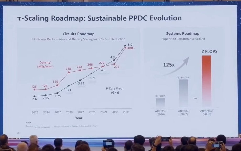
Huawei's most controversial slide. Purely technically it is not a lie, but without proper context it is misleading.
Heat is also a big problem. There's a reason major chipmakers aren't rushing to develop and produce layered chips. The main challenge, apart from purely mechanical and production challenges, is dissipating heat from them. Huawei claims that it is able to cool its new smartphone processor and at the same time speed it up compared to its predecessor. He even claims that this acceleration will continue in the coming years and after 2030 he even plans to produce chips with more than two layers. For every engineer who has had even a little to do with this issue, a red flag immediately goes off and the classic phrase “I'll believe it when I see it” comes to mind. The plan presented by Huawei, without concrete data showing how the challenges related to heat dissipation will be solved, therefore remains the riskiest part of the whole story and requires much more evidence than the declaration itself from the stage.
There are also issues related to costs (He Tingbo said that they are relatively low, but it's hard to believe in the context of the fact that two wafers are needed instead of one, which have to be tested, joined together and tested again), yield (i.e. the ratio of working chips to non-working ones), possible scale of production, etc.
The laws of physics remain the laws of physics
To sum up, Huawei has not found a way to miraculously circumvent the laws of physics or create an equivalent of the latest lithographic technologies. It has found an aggressive way to use vertical integration that allows the company to increase chip performance at relatively high cost despite the limitations just mentioned. Importantly, this method has long been known to the industry and is either already used to some extent or is part of future plans that are not treated as a priority while TSMC, Intel and Samsung are able to produce smaller and smaller transistors. The best results will still be brought by combining what Huawei is talking about with “classic” lithography progress, because these things are not mutually exclusive, and in an optimal situation they complement each other.
The above words are not an accusation against Huawei engineers. If the numbers presented by the company are true, this means in practice that In some respects, the Chinese have managed to be several years ahead of the rest of the world in terms of chip production. This is more of a complaint about marketing. And not only Chinese marketing, because similar tricks can be found in every corner of the world.
Regardless of these reservations, one thing is certain. Huawei's upcoming flagship smartphone has just become one of this year's most anticipated products, which will be taken apart around the world.