It was 1916. In a Berlin laboratory, a young chemist and metallurgist was studying the crystallization of metals. He conducted experiments and in the meantime recorded his thoughts and observations. At some point – whether from tiredness or absent-mindedness – instead of in an inkwell, he immersed the pen nib in a crucible with molten tin. When he pulled it out, a thin, silvery thread was hanging from its tip, which turned out to be a single crystal, or monocrystal. Intrigued, the scientist began to check whether this phenomenon could be repeated. He soon replaced the nib with a simple system that allowed him to dip a thin tube into molten metal and pull it out at a controlled speed, thus obtaining single-crystalline metallic rods of various sizes. This scientist was a Pole born in Kcynia, Jan Czochralskiand with his accidental discovery, he unknowingly laid the foundation for modern semiconductor production.
However, we had to wait several dozen years for this transformation from an experimental curiosity to something used on a mass scale in one of the most important industries, or more precisely, until the middle of the last century. In 1947, Bell Labs created a revolutionary device – the first transistor. Its potential was quickly discovered, so a way was needed to repeatedly obtain pure semiconductor materials with appropriate electrical parameters necessary for the production of high-quality transistors.
A replica of the first transistor. Transistors were initially made of germanium, not silicon.
|
Wikipedia.com
In connection with Bell Labs employees Gordon K. Teal and John B. Littleworked on the process of obtaining single-crystalline semiconductor rods on an industrial scale, which in practice was an extension of the Pole's experiments. In 1950, they described their work on the growth of single crystals of germanium in “Physical Review” and submitted a patent for a method and apparatus for producing germanium rods with a controlled crystal structure, which they received in 1954. However, despite their undoubted contribution to the development of technology for the production of pure single-crystalline semiconductor materials from which modern chips are made, today it is commonly called the Czochralski method (or CZ method) – thus commemorating the Polish scientist who laid its cornerstone.
Read also: Japan spends billions on semiconductors. The goal is obvious
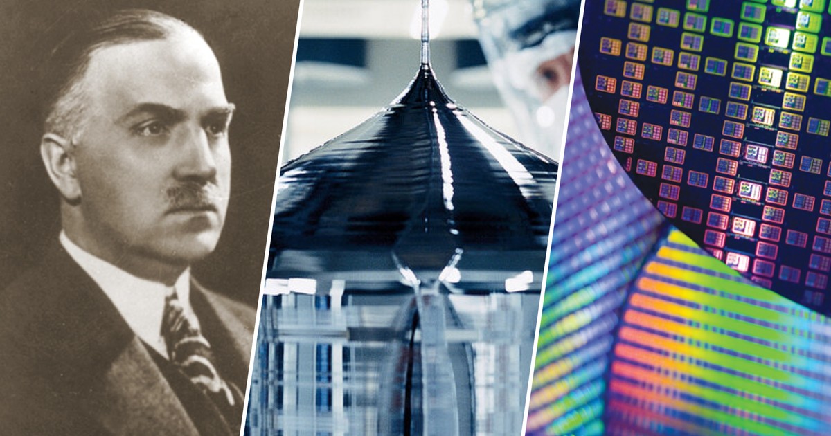
From sand to a cylinder weighing several hundred kilograms
How does it work in practice today? Since the vast majority of modern semiconductors are made of silicon, everything starts with silica, or in a sense, with sand. However, it is not ordinary sand that we can find on the Baltic Sea, but rather pure quartz (i.e. silicon dioxide). The purest quartz necessary to produce the most advanced chips is obtained in just a few places in the world. It is processed and pieces of ultrapure polycrystalline silicon are made from it.

The vast majority of the ultrapure silica that makes up the silicon wafers of the most advanced chips is mined in one place: North Carolina, USA, by Sibelco.
They go into a crucible heated to over 1,400 degrees Celsius, where they turn into a liquid. A small crystal seed touches its surface and acts as a model for subsequent atoms. As the embryo is slowly lifted, the material begins to solidify according to its structure. The forming crystal and the crucible from which it is pulled are rotated in opposite directions. By precisely regulating the rate of extraction of the forming crystal and the temperature, you can control its size.
All this is combined with advanced metrological equipment that ensures that the silicon crystal is as close to perfect as possible, because a single wafer cut from it after passing through the production line of, for example, a TSMC factory can be worth tens of thousands of dollars, and chips cut from it – millions. Factories producing the most advanced systems currently use wafers with a diameter of 300 mm, a a single monocrystalline silicon cylinder from which they are obtained can weigh from 300 to even 500 kg — definitely more than the shiny thread of tin hanging from the tip of the pen.

As a result of the Czochralski method, monocrystalline silicon cylinders are created and cut into wafers.
Attempts to erase Czochralski from history
It's safe to say that Jan Czochralski's discovery is one of the most important ones made by Polish scientists. The above description focuses on the purest version of silicon necessary for the production of modern chips, but its discovery is also used to produce photovoltaic panels or semiconductor lasers.
Unfortunately For decades, he was a completely unknown scientist in Poland, or even erased from history. In the 1920s, he gained international fame by developing and patenting in 1926 the so-called metal B, which was widely used in railways and aviation. At some point, Henry Ford invited him to cooperate, but Jan Czochralski did not accept the invitation. Instead, he accepted an invitation from Ignacy Mościcki, as a result of which he became a professor at the Warsaw University of Technology. He established the Institute of Metallurgy and Metal Science, which, among other things, developed modern methods of examining metals and which also carried out various orders from the army.
Then World War II broke out, during which he headed the laboratory of the Materials Research Department. Formally, it was subordinated to the occupiers, but its activities were a cover for conspiratorial activities, because Jan Czochralski was a collaborator of the Home Army during these years.
After the end of the war, he was accused of collaboration and although no evidence of this was found, he was not allowed to return to work at the university. Disgraced, he returned to his native Kcynia, where he opened a private company and continued his research work. He died on April 22, 1953 in a hospital in Poznańand then he was buried in his family grave.
The restoration of Jan Czochralski's place in the history of Polish science began only about 40 years laterand its culmination was in 2011, when the Senate of the Warsaw University of Technology officially cleared him of all charges. However, 2013 was, as a result of a resolution of the Sejm, the Year of Jan Czochralski, and in practice, it was only then that many Poles heard about it for the first time, although almost every engineer in any way related to semiconductors had heard about the Czochralski method for years.
Therein lies the greatest paradox of this story. Czochralski remained a forgotten figure in Poland for decades, although the world used the technology resulting from his discovery every day. Almost every smartphone, computer, car, server or satellite contains a part of that laboratory mistake from 1916. The nib dipped in molten tin was not just an anecdote from the history of science, but the beginning of a process without which the modern digital economy could not function as we know it.


